- Get Free Delivery Over 999/- On Prepaid Orders
- Use Copun "MADDY5" For 5% Instant Discount


Building a Mini Rechargeable Wi-Fi Deauther with NodeMCU, OLED & Custom PCB
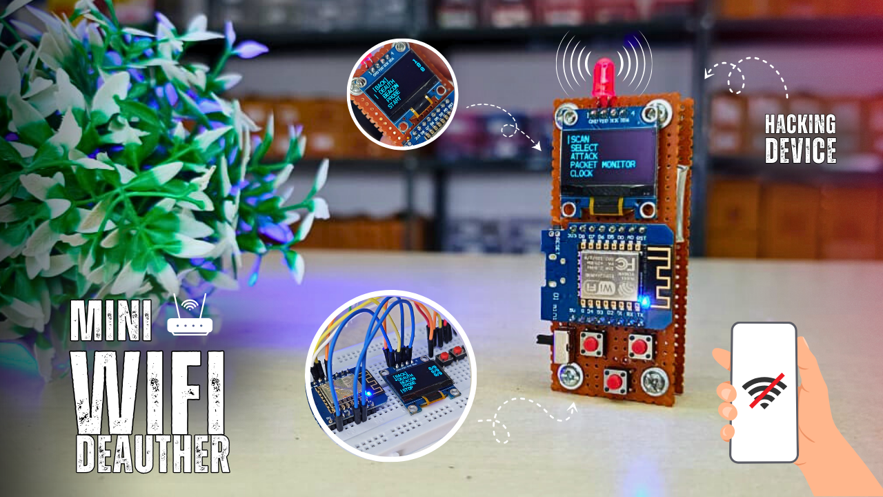
Turning a handful of parts into a compact, working gadget is deeply satisfying. This post walks the full journey from breadboard prototype to a pocketable, rechargeable device on two custom PCBs. It covers the idea, decisions, mistakes, and practical tips so you can reproduce or improve the design.
Important — Ethics & Safety (Read First)
This device can disrupt Wi-Fi networks. It is intended only for:
Learning how Wi-Fi works.
Security testing on networks you own or where you have explicit, written permission.
Controlled demonstrations in classrooms or labs.
Do not use this device to interfere with public or private networks without permission — doing so may be illegal and harmful. Always respect privacy and the law.
Why I Built This (and why you might)
I wanted a project that combined:
Embedded firmware flashing and debugging
PCB design and layout
Power management with a rechargeable cell
A compact user interface (OLED + buttons)
A tidy handheld enclosure and serviceable mechanical design
A mini Deauther is a hands-on way to learn Wi-Fi internals, RF considerations, and product-style assembly — for ethical testing and education only.
Project Overview
Core components:
NodeMCU (ESP8266 Mini) — controller
0.96″ OLED (I²C) — menu and status display
3 tactile push buttons — navigation (up, down, select)
Slide power switch — master on/off
Status LED — power/operation indicator
Single-cell Li-ion battery (3.7 V) — runtime depends on capacity
TP4056 charging module (use one with protection recommended)
Screws and spacers to stack two PCBs
Two custom PCBs: Front (UI & NodeMCU) and Back (battery & charger)
Misc: JST connector, headers, wiring, insulation, glue
Parts List (BOM)
| Part | Quantity | Notes |
|---|---|---|
| NodeMCU (ESP8266 Mini) | 1 | Choose CH340 or CP2102 USB interface variant |
| 0.96″ I²C OLED | 1 | SSD1306-compatible |
| Tactile push button | 3 | Momentary, low profile |
| Slide power switch | 1 | SPDT or SPST depending wiring |
| Status LED | 1 | 3mm or 0805 SMD with resistor |
| Li-ion single cell | 1 | Protected cell recommended |
| TP4056 charger module | 1 | With battery protection footprint or add external protection |
| JST-PH 2-pin connector | 1 | For battery connection |
| Screws & spacers | 4–6 | For stacking PCBs |
| Two PCBs (Front + Back) | 1 set | Gerbers & BOM exported |
| Misc wires, header pins, heat shrink | — | For connections and strain relief |
High-Level Workflow
Prototype on a breadboard to validate connections and firmware.
Flash firmware and verify UI/controls.
Make a quick soldered prototype on perf/vero board if needed.
Design two PCBs (front UI + back power/charger), respecting antenna keepout and decoupling.
Order PCBs, assemble, test, and finalize mechanical enclosure.
Step-by-Step Build Guide
Step 1 — Breadboard Prototype
Wire NodeMCU, OLED (I²C), three buttons, LED, and battery/charger wiring on a breadboard.
Verify USB serial connection to the PC and install required drivers if needed (CH340/CP2102/FTDI).
Ensure stable power rails: connect NodeMCU to USB 5V for prototyping or through a regulator when using battery.
Step 2 — Flash Firmware
Obtain the correct .bin firmware file.
Use an ESP8266 flasher tool:
Set default settings, select the correct COM port, select the .bin, and flash.
After flashing, reboot NodeMCU; the OLED should display the menu.
Confirm all three buttons, the slide switch, and LED work as intended.
Step 3 — Verify & Prototype PCB Path
Choose one of:
Quick solder on vero/perf board: Keep traces short, add JST for battery, expose a reflash header.
Professional PCB (Altium/other): Keep antenna keepout clear, add decoupling capacitors, test pads, mounting holes, and export Gerbers/BOM.
Step 4 — Front PCB (UI & Logic)
Place NodeMCU footprint, OLED area or cutout, button pads, slide switch, and status LED.
Provide reflash header (TX/RX/GND/3.3V) accessible after assembly.
Keep analog/digital traces short and place decouplers near NodeMCU 3.3V pin.
Step 5 — Back PCB (Power & Charger)
Footprint for battery connector and TP4056 module (or discrete charger).
Mounting holes aligned to front PCB for screws and spacers.
Keep charger and battery physically separated from RF area to reduce noise and heating issues.
Step 6 — Assembly & Mechanical Finishing
Solder small parts first (SMD passives), then larger modules and connectors.
Stack front and back PCBs with spacers and screws.
Secure battery with adhesive or a holder and use strain relief on wires.
Provide ventilation/space for TP4056—allow heat dissipation.
Step 7 — Power Up Checklist
No shorts between VCC and GND.
Switch wired correctly and tested.
Buttons, OLED, and reflash header functional.
TP4056 charging correctly, and battery polarity correct.
Step 8 — Testing
Confirm firmware boots and UI flow: boot → main menu → scan → select.
Perform only high-level, non-disruptive testing unless you have explicit permission and a controlled environment.
Log serial output for debugging; include an emergency kill switch (software and hardware) during RF tests.
Wiring / Pin Map (Breadboard → PCB)
OLED (I²C):
SDA → D2 (GPIO4)
SCL → D1 (GPIO5)
VCC → 3.3V
GND → GND
Buttons:
Up → D5 (GPIO14) (configured INPUT_PULLUP, pull to GND on press)
Down → D6 (GPIO12)
Select → D7 (GPIO13)
Status LED:
LED+ → D4 (GPIO2) via current-limiting resistor
LED− → GND
Slide Power Switch:
Switch between battery V+ and system V+ (or between battery and TP4056 output).
Battery:
JST connector to TP4056 B+ and B− pads (observe polarity)
TP4056 OUT to system 5V/3.3V path depending on your regulator design
Reflash Header:
TX/RX/GND/3.3V accessible for firmware updates
(Adjust the GPIO choices if they conflict with your OLED or NodeMCU variant. On the PCB, label pads clearly.)
Firmware & UI Expectations
Boot sequence: brief splash → main menu
Menu items might include: Scan, Attack (disabled by default unless authorized), Settings, About
Expectations for testing: From main menu select Scan → device lists APs and connected clients. If your firmware exposes RF operations, keep those functions locked behind an authorization or developer mode.
Testing and Responsible Use
What the attacks are (high level):
Deauthentication (deauth): forged management frames that tell clients to disconnect from an AP.
Beacon flooding: many fake AP beacon frames advertising bogus SSIDs to clutter the air.
Probe flooding: active probe frames to discover or provoke responses.
These summaries explain what the attacks do but do not include operational instructions.
Responsible testing rules:
Only test on equipment you own or explicitly have written permission to test.
Isolate test environment (dedicated AP, separate room or RF shielding).
Document authorization and test logs (who, when, why).
Label the device: “For authorized lab use only.”
Keep tests time-limited and include a hardware kill switch.
Lab Safety Checklist (Printable)
Written authorization for testing obtained.
Test devices and APs are physically isolated.
Emergency stop button (hardware) present and functional.
Battery polarity checked.
TP4056 module mounted with airflow for heat dissipation.
Firmware reflash header accessible for debugging.
Test log template ready (date/time, operator, device, actions, result).
Mechanical / Enclosure Notes
Design a slim front face with an OLED cutout and button holes.
Align holes for screws/spacers to stack both PCBs.
Provide a cavity or recess for the battery and a slot for USB access to the reflash header or charger port.
For 3D printing: export simple STL dimensions—hole locations, overall thickness, and insert features for switches and buttons.
Final Thoughts and Next Steps
This build teaches firmware, UI design, power management, PCB layout, and mechanical finishing. The split-PCB approach (front UI + back power) keeps noisy power electronics away from RF/UI and simplifies maintenance.
If you want, I can:
Create a wiring diagram with a clear pin map and breadboard-to-PCB transitions.
Make a step-by-step photo assembly guide formatted for your blog.
Draft basic STL measurements for a 3D printed case.
Reformat this post to match your blog’s voice/length and add headings or callout boxes.
Recent Comments
Posts Widget
Subscribe Us
Need Help?
Monday – Friday: 9AM-6PM
Saturady & Sunday: 11:00 – 15:00
Important Links
- 🚀 Genuine Products, Guaranteed Trust
- ⚡ Fast Delivery, Every Time
- 🤝 Best Support, Always Here
- 🔒 Secure Payments, Worry Free
Copyright 2025 ©MaDDy Electronics. All right reserved By MaDDy Electronics
